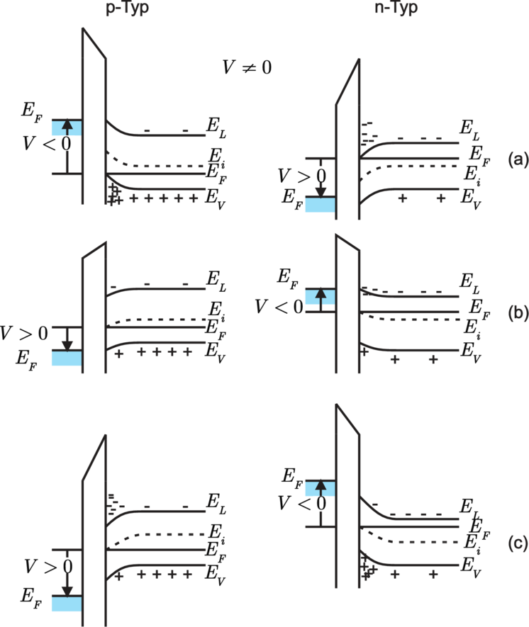
38 schottky diode band diagram
PDF Chapter three schottky contact diode fabrication Figure 7: Schottky diode with energy band diagram showing the reverse bias Va applied to the diode that increases the built-in potential. 6. Aspects that affect the magnitude of current through the ideal Schottky diode are the area (A) of the metal contacting the semiconductor, the temperature (T) of the... PDF Broadband schottky diode 2 Schottky Diode Technology for Frequency Multipliers. 145 5.9 Block diagram for the W -band fundamental mixer measurement. . . . 145 5.10 Measured output power across W -band for 100 mW input power. . . .
Category:Schottky diode diagrams - Wikimedia Commons Category:Schottky diode diagrams. From Wikimedia Commons, the free media repository. Jump to navigation Jump to search. Band Diagram of Schottky Barrier Detector.png 696 × 489; 69 KB.

Schottky diode band diagram
Schottky Diode - an overview | ScienceDirect Topics The energy band diagram for a Schottky barrier diode formed at a metal/n-type semiconductor interface is displayed in Fig. 17.2 . At zero bias ( Fig. 17.2 A), the redistribution of electrons to reach an equilibrium state creates a space charge region in the semiconductor with a width given by. Schottky Diode Characteristics and Its Applications Schottky Diode Diagram. It is well known that there are a large amount of conductive electrons inside a metal conductor. When the metal is in contact with the semiconductor (the distance between them is only an atom), the Fermi level of the metal is lower than the Fermi level of the semiconductor, and the... Schottky Diode or Schottky Barrier Semiconductor Diode Schottky diodes have many useful applications from rectification, signal conditioning and switching, through to TTL and CMOS logic gates due mainly to their low power and fast switching speeds. TTL Schottky logic gates are identified by the letters LS appearing somewhere in their logic gate circuit...
Schottky diode band diagram. Schottky Diode Symbol, Applications, Advantages - ETechnoG The advantages of Schottky diode over Normal PN junction Diode are high switching speed, no reverse recovery time. Schottky Diode is an advanced version of normal PN Junction diode having a lot of advantages and important applications. Schottky Diode | 2. Flatband diagram and built-in potential In a Schottky diode, the semiconductor band diagram looks very similar to that of an n-type semiconductor in a p+-n diode (compare Fig. 1a and 2). Hence, the variation of the space charge density, r, the electric field, F, and the potential, f, in the semiconductor near the metal-semiconductor... PDF Using modern semiconductor fabrication processes, the... Energy band diagram of metal and semiconductor separate from each other when semiconductor surface states exist. Schottky diodes have been fabricated with cutoff frequencies greater than 1 THz. In general, a diode can be used at frequencies less than fc/10. Schottky Diode - Characteristics, Parameters and Applications Schottky diode is another type of semiconductor diode, but instead of having a P-N junction, Schottky diode has a metal-semiconductor junction and which reduces capacitance This schematic symbol can easily be used to distinguish Schottky diode from other diodes when reading a circuit diagram.
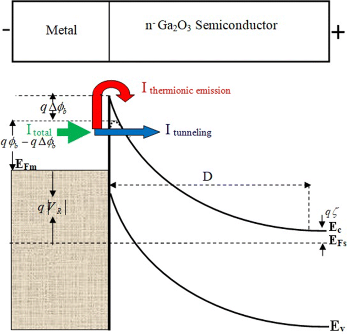
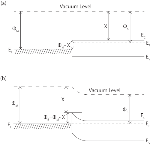
Schottky Diode - Function, Construction, Characteristics, Applications... A Schottky diode, widely popular as barrier diode, refers to a metal-semiconductor diode that comprises lower voltage drops than usual PN-junction diodes. The following diagram represents the Schottky diode symbol -. [Image will be Uploaded Soon]. In the above diagram, the anode section... An Overview of the Ultrawide Bandgap Ga2O3 Semiconductor-Based... Schottky Barrier Diode Based on β-Ga2O3. The difficulties in the growth of high-quality and low-cost single-crystal substrates have affected the a Schematic of the cross-sectional Pt/Ga2O3 SBD and p-Cu2O/n-Ga2O3 diode. b Band diagram of the p-Cu2O/n-Ga2O3 interface. c, d Forward and reverse... Schottky Diode: Technology & Structure » Electronics Notes Schottky Barrier Diode Tutorial Includes: Schottky barrier diode Schottky diode technology Schottky diode specs Schottky diode power rectifier. Whilst the early Schottky diodes were very straightforward, the basic technology has been developed to enable both small signal and power... Metal-Semiconductors Contacts - Engineering LibreTexts Figure 1 shows the energy band diagram after the contact is made. Not all MS contact can perform as the rectifying Schottky diode, since there is no potential barrier formed. Under this situation, when the current can be conducted in both directions of the MS contact, the contact is defined as the Ohmic...
PDF Graphene Schottky diodes: an experimental review of the rectifying... Schottky diodes are important electronic components, used in many applications such as solar cells, photodetectors, clamped transistors, MESFETs equilibrium band diagram for the M/S junction. The physical junction is set at x = 0 . Fi is the energy. barrier to the flow of electrons (black dots) from the... Schottky Diode Part 1 - Band Diagram - YouTube Schottky Diode Part 1 - Band Diagram. Energy band diagram of a metal-semiconductor Schottky diode with... Schottky Diodes, Channels and Bias (Epidemiology) | ResearchGate, the professional network for scientists. Near-infrared radiation of wavelength 1.5 μm is up-converted to a visible wavelength of 818 nm by internal photoemission in a Schottky diode with a modulation p-doped channel. Schottky Diode Working and Its Applications Schottky diode is also known as barrier diode. Learn more about Schottky diode working, construction, V-I characteristics, features and Due to thermal agitation, some carriers have equal energy to or larger than the conduction band energy to the metal-semiconductor interface, and to the...
Electric dipole effect in PdCoO2/β-Ga2O3 Schottky diodes for ...
Schottky diode - encyclopedia article - Citizendium The Schottky diode is a two-terminal device consisting of conductive gate (for example, a metal) on top of a semiconductor body. It is named after Walter H Schottky, who proposed a detailed theory for point contact rectification in 1938.

Schottky-Diode - Wikiwand
Schottky Diode - Electronics-Lab.com The Schottky diode is a semiconductor diode formed by the junction of metal with the semiconductor material. The Schottky diode is also known as a hot-carrier diode and Schottky barrier diode. It has a low forward voltage drop and high switching speed.
Band diagram of a Schottky diode on n-type silicon ...
Introduction to Schottky diode - projectiot123 Technology Information... Schottky diode also known as the hot carrier diode is a two terminal passive electronic component and a special purpose diode. Schottky diode is the high speed device due to its specially designed junction and thus is employed in high speed applications.
BJNANO - Monolayer graphene/SiC Schottky barrier diodes with ...
Schottky Diodes - Working, Characteristics, Application - Homemade... Schottky diodes are constructed differently compared to the traditional p-n junction diodes. Instead of a p-n junction they are built using a metal In Schottky diodes electrons become the majority carrier in the semiconductor material, while in the metal exhibits extremely small minority carriers (holes).
Schottky Diodes Heterojunctions and NDR Diodes
Диод шоттки: принцип работы и сферы его применения, чем... . . .

a) Energy band diagram of Back-to-Back Schottky diodes with a ...
Schottky diode - Wikipedia The Schottky diode (named after the German physicist Walter H. Schottky), also known as Schottky barrier diode or hot-carrier diode, is a semiconductor diode formed by the junction of a semiconductor with a metal. It has a low forward voltage drop and a very fast switching action.

Schottky Diodes (M-S Contacts)web.it.nctu.edu.tw/~thhou/12 ...
Schottky Diode: What is it? (Symbol, Applications...) | Electrical4U A SIMPLE explanation of Schottky Diodes (hot-carrier diode or Schottky barrier diode). Learn what a Schottky Diode is, the symbol for a Schottky Diode Schottky diodes have a low forward voltage drop (0.15 to 0.45 V) and a very fast switching action. Just like a regular diode, a Schottky diode will...
1 ECE 305 Homework SOLUTIONS : Week 9 Mark Lundstrom Purdue ...
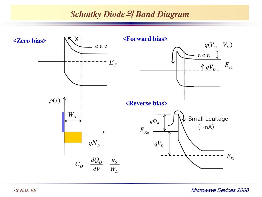
PDF Thermal characterization of THz planar Schottky diodes using... Schottky diodes are preferred and used in heterodyne receivers as a mixing element. In higher frequencies (THz band) the size of the diode The energy band diagram of metal-semiconductor (n-type) in forward and reversed bias looks like Figure 2.2 which is further described in [10] and not...

Schottky Barrier Diode - Power Microelectronics. Device and ...
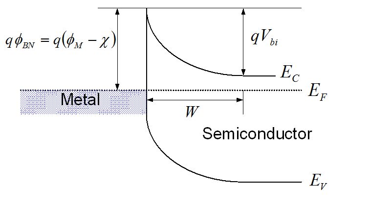
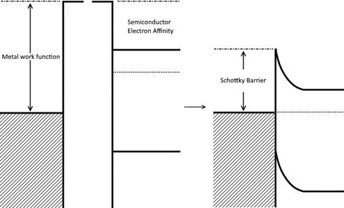
Energy band diagram of schottky diode Schottky diode is also known as schottky barrier diode, surface barrier diode, majority carrier device, hot-electron diode, or hot carrier diode. The energy band diagram of the N-type semiconductor and metal is shown in the below figure. The vacuum level is defined as the energy level of electrons that...
Why does the SiC Schottky barrier diode (SBD) have a high ...
PDF Schottky Diode Schottky Diode. Features: • Low power loss, high efficiency • High current capability, low VF • High reliability • High surge current : DO-41 moulded plastic : Pure tin plated, lead free, solderable per MIL-STD-202, Method 208 guaranteed : Colour band denotes cathode end : 260°C/10 seconds/0.375"...
Schottky Diode or Schottky Barrier Diode | ProtonsTalk
What is a Schottky Diode? A schottky diode is a diode that has a low forward voltage drop and a very fast switching ability. A schottky diode, however, is made from a metal semiconductor junction. This metallic junction, which is more conductive, allows for easier conduction across than with a typical PN junction.
Schottky diode
Schottky Diode or Schottky Barrier Semiconductor Diode Schottky diodes have many useful applications from rectification, signal conditioning and switching, through to TTL and CMOS logic gates due mainly to their low power and fast switching speeds. TTL Schottky logic gates are identified by the letters LS appearing somewhere in their logic gate circuit...

Modeling Electrical Properties of Organic Schottky Diodes ...
Schottky Diode Characteristics and Its Applications Schottky Diode Diagram. It is well known that there are a large amount of conductive electrons inside a metal conductor. When the metal is in contact with the semiconductor (the distance between them is only an atom), the Fermi level of the metal is lower than the Fermi level of the semiconductor, and the...

Schottky diode - Definition, Symbol, Working and Applications ...
Schottky Diode - an overview | ScienceDirect Topics The energy band diagram for a Schottky barrier diode formed at a metal/n-type semiconductor interface is displayed in Fig. 17.2 . At zero bias ( Fig. 17.2 A), the redistribution of electrons to reach an equilibrium state creates a space charge region in the semiconductor with a width given by.

Energy band diagram of Schottky diode with n-type base and DL ...

Research Express@NCKU - Articles Digest (Volume 9 Issue 8)
Implementation of Schottky Barrier Diodes (SBD) in Standard ...
Combined thermionic emission and tunneling mechanisms for the ...

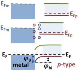
Ohmic Contacts, Schottky Barriers and Schottky Diodes ...

Extraction of the Schottky parameters in metal-semiconductor ...
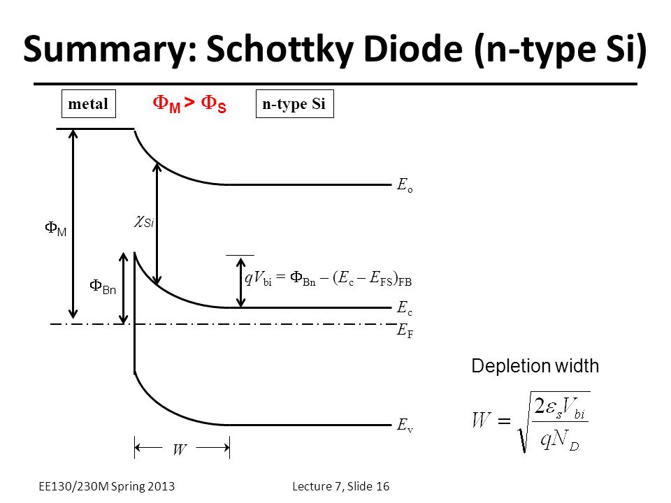
Lecture 7 OUTLINE Poisson's equation Work function Metal ...

Schottky Diode or Schottky Barrier Semiconductor Diode
Schottky diode - encyclopedia article - Citizendium

Porous Ag/TiO2-Schottky-diode based plasmonic hot-electron ...

Figure 2 from On the Influence of Surface Treatment on ...

Flexible carbon nanotube Schottky diode and its integrated ...

Metal–semiconductor junction - Wikipedia

Schottky Barrier - an overview | ScienceDirect Topics
Schottky Barrier

EE327 Lec 22c Schottky
Phanomene elektrischer Kontakte
GaN-Based Schottky Diode | IntechOpen
Microwave Devices - Microwave Semiconductor Devices ppt download
![PDF] Graphene Schottky diodes: an experimental review of the ...](https://asset-pdf.scinapse.io/prod/1872496776/figures/figure-1.jpg)
PDF] Graphene Schottky diodes: an experimental review of the ...

Electric dipole effect in PdCoO2/β-Ga2O3 Schottky diodes for ...

Layer dependence and gas molecule absorption property in MoS2 ...

InSe Schottky Diodes Based on Van Der Waals Contacts - Zhao ...
Metal oxide semiconductor-based Schottky diodes: a review of ...
0 Response to "38 schottky diode band diagram"
Post a Comment